This page provides basic information about voltage comparator integrated circuits and is to act as reference material for other circuits. The circuits shown are based on the LM339 Quad Voltage Comparator chip or the LM393 Dual Voltage Comparator chip. These devices are functionally identical. The LM311 Voltage Comparator can be used for these applications as well and also has a number of unique features.
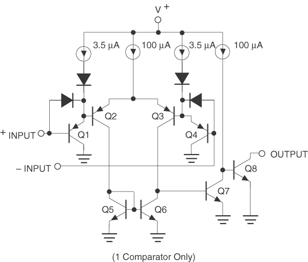
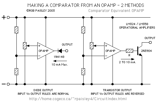
An integrated circuit "Voltage Comparator" is equivalent to an Operational Amplifier, Such as the LM358 or LM324, with two NPN transistors added to the output of each amplifier. (Refer to the above schematic.) This arrangement produces an "Open Collector" output for each of the four comparators in an LM339 chip. Each output can sink up to 20Ma and can withstand voltages of up to 50 Volts.
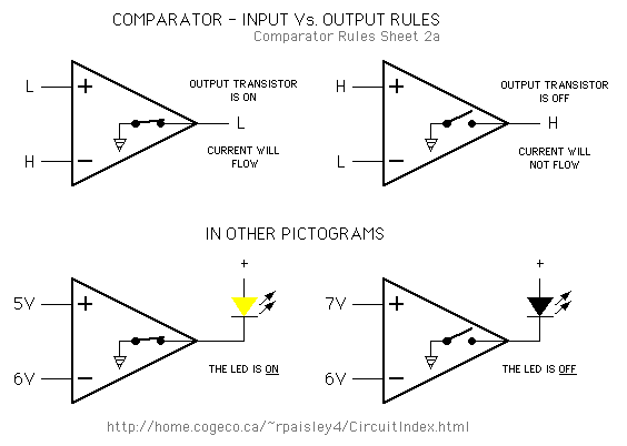
The output is switched ON or OFF depending on the relative voltages at the PLUS and MINUS inputs of the comparator, see the rules below. The inputs are quite sensitive and a difference of only a few millivolts between the two will cause the output to turn on or off.
The LM339, LM393 and LM311 comparator chips can operate from a single or dual power supply of up to 32 volts maximum.
When operated from Dual or Split power supplies the basic operation of comparator chips is unchanged except that for most devices the emitter of the output transistor is connected to the negative supply rail and not the circuit common. An exception to this is the LM311 which has a separate emitter terminal that can be connected to either.
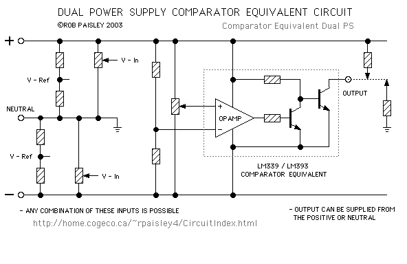
When operated from Dual or Split power supplies the input voltages can be above or below the common or zero voltage of the supply. If needed, one of the inputs can be connected to the common so that a 'Zero Crossing' detector is created.
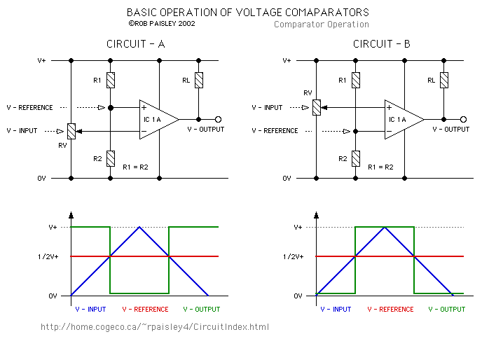
The following drawing show the two simplest configurations for voltage comparators. The diagrams below the circuits give the output results in a graphical form.
For these circuits the REFERENCE voltage is fixed at one-half of the supply voltage while the INPUT voltage is variable from zero to the supply voltage.In theory the REFERENCE and INPUT voltages can be anywhere between zero and the supply voltage but there are practical limitations on the actual range depending on the particular device used.
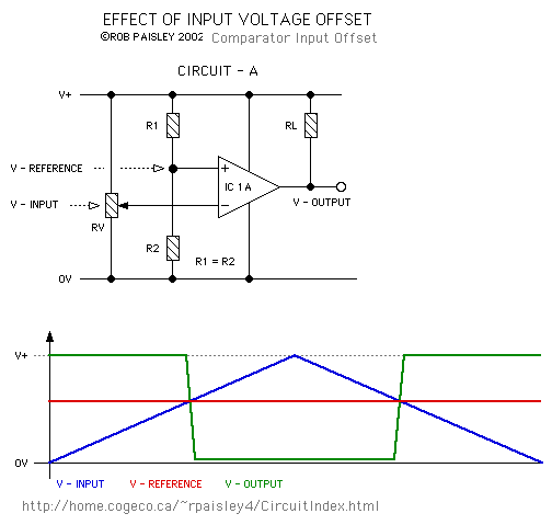
Voltage comparators are not perfect devices and in some instances may suffer from the effects of a parameter known as the Input Offset Voltage. This problem normally occurs when the Input voltage changes very slowly. The Input Offset Voltage for many comparators is only a few millivolts and in most circuits it can be ignored.
The net result of the Input Offset Voltage is that the output transistor does not fully turn on or off when the input voltage is close to the reference voltage.
The following diagram attempts to illustrate the effect of the input offset voltage with a slowly changing input voltage. This effect increases as the output transistor current increases so keeping the value of RL high will help reduce the problem.
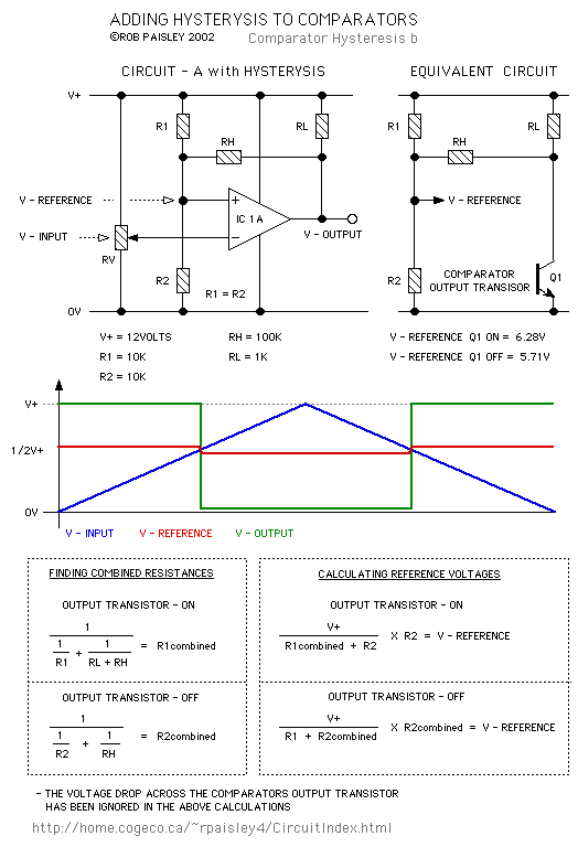
The effects of the input offset voltage can be countered by adding hysterysis to the circuit. This causes the reference voltage to change when the comparators output goes high or low.
The effect is that as the input voltage slowly changes the reference voltage will quickly change in the opposite direction. This gives the comparator a "snap" action. See the following paragraphs for more information.
Hysteresis is the difference between the input signal levels at which a comparator turns off and turns on. A small amount of hysteresis can be useful in a comparator circuit because it reduces the circuit's sensitivity to noise, and helps reduce multiple transitions at the output when changing state.
Sometimes, in a discrete design, there is a need to add an external resistor between the comparator's output and the positive input, creating a weak positive feedback loop. When the output makes a transition, the positive feedback slightly changes the positive input so as to reinforce the output change.
A mechanical analog of this effect can be found in many electrical switches. As you move the handle just past the center point, a spring in the switch will try to pull the handle all the way over, ensuring that the switch ends up in a definite ON or OFF state.
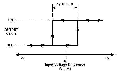
The diagram above shows a hysteresis 'loop' that describes how a comparator functions. The horizontal 'X' axis is the input, and represents the difference of the two input voltages. The vertical "Y" axis represents the comparator's output state.
If the comparator is initially 'OFF', the MINUS input voltage has to become slightly above the PLUS input voltage before the comparator output turns 'ON'. This is represented by moving right along the bottom part of the loop.
Once the comparator is 'ON', the MINUS input voltage needs to drop slightly below the PLUS input voltage before it turns 'OFF' again (moving left along the top of the loop).
The width of the loop outlined by an off-on-off cycle is the input hysteresis voltage.
The hysteresis voltage for most comparators is in the millivolt range and usually only affects circuits where the input voltage rises or falls very slowly or has voltage spikes knoown as "noise".
The Hysterysis voltage range can be increased if needed to help when the input voltage is noisey so the the output does not change states unnecessarily. The FLIP-FLOP circuits shown later on this page make use of an exaggerated hysterysis to create the memory effect.
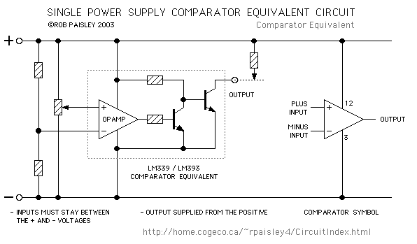
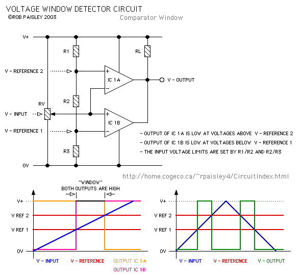
Comparators with Open Collector outputs such as the LM339 or LM393 must be configured so the both outouts are HIGH when the voltage is within the desired limits. The LM311 comparator can have other output arrangements as it has both an open collector and open emitter on the output transistor.
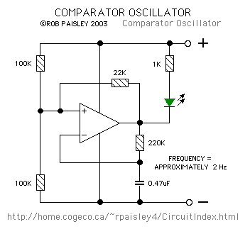
Comparators can also be used as oscillators but are not particularly well suited for this use.
If there are Operational Amplifiers left over in a circuit and a Comparator is needed one can be created by adding a diode or transistor to the amplifiers output depending on the current capacity required.
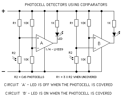
The following diagrams are of some basic comparator circuits. Most have a Cadmium Sulfide photocell input but could just as easily use a phototransistor or a voltage signal from another circuit as an input. The resistance values are not critical but should be used as a guide. In most comparator circuits the ratio of the resistances is more important than their actual values.
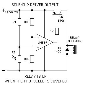
If higher current loads are to be driven a PNP transistor can be added to the comparators output this will allow loads of up to 300Ma. to be controlled.
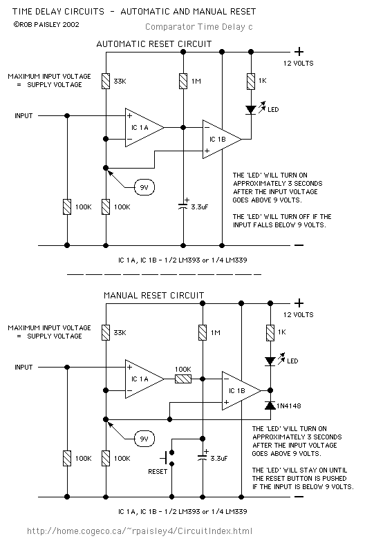
Short timing functions such as a pulsed outputs or time delays can also be created with one or two comparator sections.
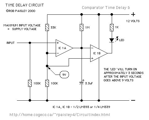
Notice that the second comparator section in the time delay circuit shares the same reference voltage input as the first. In most cases any number of comparators can have the same voltage source at one input, this can make circuits much less complicated.
More Delay circuits.
Comparators can be made to perform a basic memory function by wiring them as a 'SET / RESET' type of FLIP/FLOP. This type of circuit can be used in unplugable walk around throttles to remember the direction of the train when the controller is disconnected. In the next diagram the comparator will remember which switch was pushed last. If the 'SET' button is pushed the LED will be on, the 'RESET' button will turn the LED off. A higher current version is also shown.
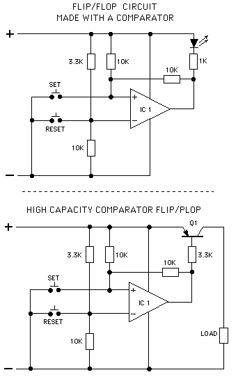
How the Flip Flop works. A very basic description.
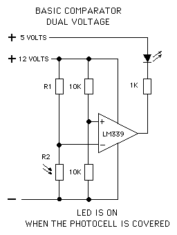
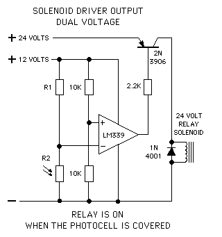
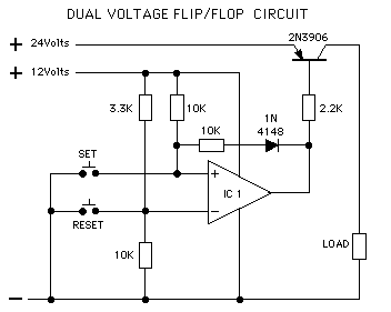
Because the output transistor of the comparator has an open collector the supply and load voltages do not have to be the same. This means that the comparator could use a 12 Volt power supply while the load could be a 24 Volt relay or 5 Volt LED circuit.
The following three diagrams are some examples of Dual voltage circuits. In the first two the voltage at the output of the comparators could even be full wave direct current.
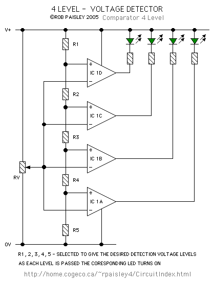
This circuit can sequentially indicate 4 separate voltage levels. The voltages are determined by the values of resistors R1 through R5 arranged in a simple voltage divider circuit.